We work on cryogenic and computational electron microscopy, and we are also very interested in applying these approaches to functional material systems. Extending these methods to real-world samples often requires additional experimental and computational development, and much of this work happens through close collaboration. See the User Highlights page for a few examples of how we have applied these methods in practice.
Cryo-EM
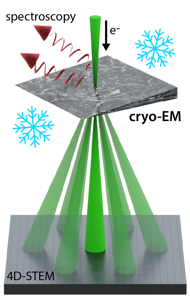
We develop novel cryogenic electron microscopy techniques, with an emphasis on convergent-beam scanning transmission electron microscopy (STEM) approaches for materials science samples. These methods are applicable to electron beam-sensitive materials, including soft matter, polymers, biological structures, and next-generation energy technologies. They also allow us to observe low-temperature phenomena in materials, including phase transitions and ordering in quantum materials. This research will be conducted at cryoEPIC (Cryo Electron Ptychography and Imaging Center), a new cryo-EM facility at Berkeley Lab for research at the intersection of materials science and biological sciences.
Computational Imaging
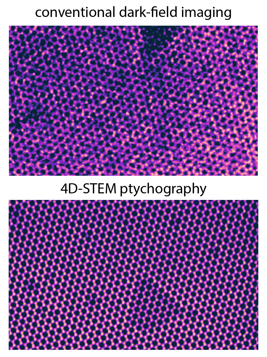
Combining computational imaging with electron microscopy experiments enables characterization not possible with conventional techniques. We develop computational methods and integrate them with data acquisition and analysis, from automation to offline data processing. Many of these methods leverage 4D-STEM, including nanobeam diffraction and diffractive imaging techniques such as ptychography. We are especially interested in coupling 4D-STEM with complementary approaches, including tomography, spectroscopy, and in situ methods. Visit our Open-Source Code page to learn more about the computational tools that we are developing.